From https://www.ynetnews.com/business/article/bjm6vfjwgx
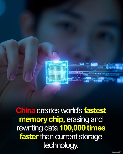
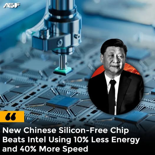
Chinese scientists have developed what they call "the fastest, most efficient transistor ever"— and it contains no silicon at all. Built using ultra-thin sheets of bismuth, the new transistor outperforms the best silicon-based processors produced by leading manufacturers such as Intel and TSMC — the same Taiwan-based company that builds chips for Apple.
The groundbreaking development, published by Nature Materials in February, represents a radical departure from current chip design. Instead of trying to improve existing technologies, the team led by Prof. Peng Hailin at Peking University chose an entirely novel path.
“If chip innovations based on existing materials are considered a ‘short cut’, then our development of 2D material-based transistors is akin to ‘changing lanes’,” Peng told the South China Morning Post.
A shift from 'fins' to 'bridges'
To understand the significance of the breakthrough, it’s crucial to consider what it replaces. Since the early 1990s, most transistors — the tiny switches that drive everything from smartphones to supercomputers — have relied on silicon and a structure known as the Fin Field-Effect Transistor, or FinFET. These vertical, skyscraper-like structures provide better control over electric current at the nanoscale.
But FinFETs are reaching their physical limits. As chip sizes shrink below 3 nanometers, engineers face mounting challenges in improving performance while keeping power consumption in check. So instead of shrinking the old design, Peng and his team abandoned it entirely.
The new transistor uses a 2D gate-all-around field-effect transistor (GAAFET). Unlike FinFETs, which wrap the gate around three sides of the transistor’s channel, GAAFETs surround it on all four sides. This provides better current control and drastically reduces energy loss. Yet the real breakthrough lies not in the structure, but in the materials used.
Bismuth beats silicon
Rather than silicon, the researchers used bismuth oxychalcogenide for the transistor’s channel and bismuth selenide oxide for the gate material. These belong to a class of atomically thin materials known as two-dimensional semiconductors, which have extraordinary electrical properties.
Bismuth oxychalcogenide, in particular, offers advantages that silicon struggles with at extremely small scales. Electrons move faster through it, even when tightly packed, and it has a higher dielectric constant, meaning it can hold and control electric charge more efficiently. That translates into faster switching, lower energy loss and less heat generation.
“This reduces electron scattering and current loss, allowing electrons to flow with almost no resistance, akin to water moving through a smooth pipe,” Peng explained. In practical terms: less friction, less heat and more performance for less power — a dream for any smartphone user.
Up to 40% faster with 10% less energy
The lab results are striking. According to the research team, their transistor can operate up to 40% faster than today’s most advanced 3-nanometer silicon chips, while using 10% less energy.
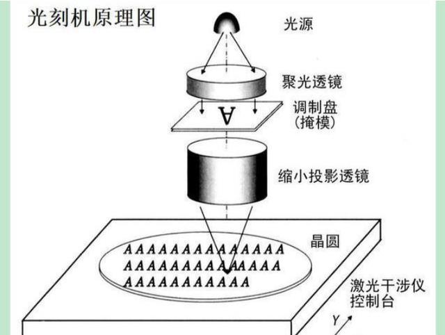
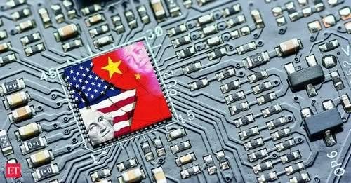
The motivation behind the innovation is not just technical, but geopolitical. As a result of ongoing U.S. sanctions, Chinese firms are unable to purchase the cutting-edge equipment required to manufacture advanced silicon chips. The most sophisticated lithography machines, essential for producing 3-nanometer chips, are made by a handful of Western companies such as ASML in the Netherlands.
By creating a transistor that doesn’t depend on silicon — and that can be fabricated using equipment already available in China — Peng’s team may have found a way to bypass those export controls. “While this path is born out of necessity due to current sanctions, it also forces researchers to find solutions from fresh perspectives,” Peng said.
Global race for post-silicon chips
China isn’t alone in seeking alternatives beyond silicon. IBM has been developing carbon nanotube technologies for years, while Intel is exploring experimental chip packaging methods to overcome miniaturization limits. TSMC, the industry leader, continues to refine its chip designs in the race to maintain its dominance.
Despite the promising lab performance, major questions remain. Can these transistors be produced at scale? Will they withstand the heat and stress of real-world usage, in smartphones or gaming PCs? And how soon could this technology reach consumer devices?
Peng said his team is already working on scaling up production. Early prototypes of logic units built using the transistor showed exceptionally low operating voltages. Their use of existing manufacturing platforms suggests that mass production barriers may be lower than with other experimental technologies.
“This work demonstrates that 2D GAAFETs do exhibit comparable performance and energy efficiency to commercial silicon-based transistors, making them a promising candidate for the next technology node,” Peng wrote in the paper.
Still, turning lab breakthroughs into commercial chips typically takes years, sometimes decades. Designing a single transistor is one thing; integrating billions of them into a reliable, mass-produced chip is another. But if successful, this could give China a critical new foothold in the global chip race.
More broadly, the breakthrough signals that the semiconductor race may no longer be about who can shrink silicon the most, but who can think beyond it.
Author: Saikat Bhattacharya